Buku Persamaan Ic Dan Transistor Amplifier Circuits
Contents • • • • • Overview [ ] ' as the term is currently used refers to a monolithic IC which differs notably from a HIC in that a HIC is fabricated by inter-connecting a number of components on a substrate whereas an IC's (monolithic) components are fabricated in a series of steps entirely on a single wafer which is then diced into chips. Some hybrid circuits may contain monolithic ICs, particularly (MCM) hybrid circuits. Hybrid circuits are often encapsulated in, as shown in the photo. A hybrid circuit serves as a component on a PCB in the same way as a monolithic; the difference between the two types of devices is in how they are constructed and manufactured. The advantage of hybrid circuits is that components which cannot be included in a monolithic IC can be used, e.g., capacitors of large value, wound components, crystals, inductors. Is often used as the interconnecting medium for hybrid integrated circuits.

The use of screen printed thick film interconnect provides advantages of versatility over thin film although feature sizes may be larger and deposited resistors wider in tolerance. Multi-layer thick film is a technique for further improvements in integration using a screen printed insulating dielectric to ensure connections between layers are made only where required.
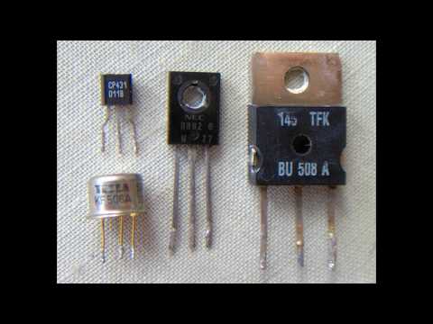
Simple audio amplifier circuit diagram using transistor. Buku persamaan ic dan transistor amplifier with symbol staffengineer. Test po linejnoj algebre.
One key advantage for the circuit designer is complete freedom in the choice of resistor value in thick film technology. Planar resistors are also screen printed and included in the thick film interconnect design.
The composition and dimensions of resistors can be selected to provide desired values. The final resistor value is determined by design and can be adjusted. Once the hybrid circuit is fully populated with components, fine tuning prior to final test may be achieved by active laser trimming. Thin film technology was also employed in the 1960s. Ultra Electronics manufactured circuits using a silica glass substrate. A film of tantalum was deposited by sputtering followed by a layer of gold by evaporation.
The gold layer was first etched following application of a photo resist to form solder compatible connection pads. Resistive networks were formed, also by a photo resist and etching process. These were trimmed to a high precision by selective adonization of the film. Capacitors and semiconductors were in the form of LID (Leadless Inverted Devices) soldered to the surface by selectively heating the substrate from the underside. Completed circuits were potted in a diallyl phthalate resin.
Several customized passive networks were made using these techniques as were some amplifiers and other specialized circuits. It is believed that some passive networks were used in the engine control units manufactured by Ultra Electronics for Concorde. Some modern hybrid circuit technologies, such as -substrate hybrids, allow for embedding of components within the layers of a multi-layer substrate in addition to components placed on the surface of the substrate. This technology produces a circuit that is, to some degree,. Steps in manufacturing Solid Logic Technology hybrid wafers used in the and other IBM computers of the mid-1960s. The process starts with a blank ceramic wafer 1/2 inch square.